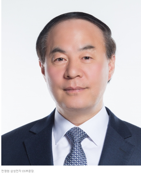
The Samsung Semiconductor Division has faced significant challenges over the past few years. With Jeon Young-hyun recently marking his 100th day as head of the Device Solutions (DS) Division, he has been focused on recovering fundamental technological competitiveness and driving organizational cultural innovation. This blog will delve deeply into the current situation at Samsung and analyze the strategic challenges that lie ahead for Jeon and his team.

1. Restoring Technological Competitiveness: The Key Role of HBM3E and HBM4
Restoring technological competitiveness is crucial for Samsung as it seeks to reclaim its leadership in the semiconductor market. Particularly in the memory semiconductor segment, where competition has intensified, maintaining a technological edge is critical for both market share and profitability. Jeon Young-hyun, recognizing this, has made the recovery of technological competitiveness a cornerstone of his strategy, with a particular focus on High Bandwidth Memory (HBM) technologies such as HBM3E and HBM4.
The Importance of HBM3E Development
HBM3E is one of the most important technologies that Samsung is currently focusing on. High Bandwidth Memory is crucial for high-performance computing, AI, and graphics cards, which require fast data processing capabilities. In this space, competitors like SK Hynix and Micron have been advancing rapidly, and Samsung has struggled to maintain its lead.
To address this, Samsung is accelerating the development of HBM3E, aiming to supply it to key customers like AMD and several AI semiconductor startups. However, the real test lies in securing a supply agreement with NVIDIA, the dominant player in the AI accelerator market, controlling over 95% of it. Successfully securing a deal with NVIDIA would be a significant win for Samsung, solidifying its position in the HBM market.
Samsung has already succeeded in supplying HBM3 to NVIDIA, and there is a high likelihood that it will also supply HBM3E. However, the critical factors will be the timing and volume of the supply. If Samsung can supply HBM3E 12-layer products to NVIDIA before its competitors, it could dramatically shift the competitive landscape in its favor. Conversely, if it falls behind, with SK Hynix maintaining its lead, Samsung might struggle to secure significant market share, which could limit its influence in the AI accelerator market.
HBM4: A Strategic Gamble for the Future
While HBM3E is key to short-term technological competitiveness, HBM4 is poised to play a critical role in Samsung's long-term strategic positioning. HBM4 is expected to offer significantly improved performance over its predecessor, making it essential for meeting the demands of AI, high-performance computing, and next-generation computing markets.
One of the key aspects of HBM4 development is the involvement of Samsung's foundry business in producing the logic die. This integration allows Samsung to capitalize on its vertical integration, producing both the memory and the logic die, which could offer significant performance advantages and cost efficiencies. This capability could set Samsung apart from its competitors, especially as SK Hynix has partnered with TSMC for their logic die production.
The success of HBM4 will not only reinforce Samsung's position in the memory semiconductor market but also create synergies across its business units, particularly between its memory and foundry divisions. This synergy is crucial as the importance of advanced packaging technologies grows, especially in connecting GPUs, HBM, and CPUs in high-performance systems.
The Broader Significance of Restoring Technological Competitiveness
Jeon Young-hyun's emphasis on restoring technological competitiveness is about more than just gaining market share—it’s about securing Samsung's future in the semiconductor industry. The development of HBM3E and HBM4 is central to this strategy, as these technologies are not only pivotal in maintaining Samsung's leadership in the memory market but also in re-establishing the company as a leader in semiconductor innovation.
Restoring this competitiveness is essential not just for short-term revenue growth but for securing long-term leadership in an industry where technology evolves rapidly. For Samsung to close the gap with its competitors and reassert its dominance, these technological advancements must succeed.
2. Organizational Restructuring and Strategic Shifts: Maximizing Synergy and Addressing Risks
Jeon Young-hyun's leadership of Samsung's Device Solutions (DS) division has been marked by significant organizational restructuring aimed at boosting efficiency, fostering innovation, and maximizing synergy across different segments of the business. These changes are not just routine adjustments but strategic maneuvers designed to address the critical challenges Samsung faces in the highly competitive semiconductor industry. In this section, we will explore the key aspects of this restructuring, its strategic implications, and the potential risks involved.
Establishing the HBM Development Team: Focusing on Technological Excellence
One of the most prominent moves in Jeon’s restructuring plan was the establishment of a dedicated High Bandwidth Memory (HBM) development team within the DRAM Development Division. Previously, expertise in HBM was dispersed across various task forces within the company, which may have led to inefficiencies and slower progress in technological development. By consolidating this expertise under one roof, Samsung aims to accelerate innovation and enhance its competitiveness in the HBM market, where it has been facing stiff competition from rivals like SK Hynix and Micron.
The creation of this dedicated team signifies Samsung’s commitment to leading in HBM technology, which is critical for high-performance computing (HPC), artificial intelligence (AI), and advanced graphics processing units (GPUs). The centralized focus on HBM development is expected to yield faster advancements and better integration of new technologies, allowing Samsung to potentially outpace its competitors in delivering cutting-edge memory solutions to the market.
This restructuring move also reflects a broader strategy to enhance efficiency and collaboration within the company. By bringing together top talent and resources in HBM under one team, Samsung can foster a more focused and cohesive approach to developing next-generation memory technologies, which are essential for maintaining its leadership in the semiconductor industry.
Integrating Research and Development Units: Enhancing Process Efficiency
Another significant organizational change under Jeon’s leadership was the integration of the Semiconductor Research Center with parts of the Equipment Technology Research Center. The latter was previously responsible for the development of eight core process equipment technologies, a crucial aspect of semiconductor manufacturing.
This integration is designed to create closer collaboration between process development and equipment technology teams, ultimately improving the efficiency of Samsung's semiconductor manufacturing processes. By aligning these functions more closely, Samsung aims to streamline the development process, reduce time-to-market for new technologies, and enhance the overall efficiency of its manufacturing operations.
This restructuring is particularly important in an industry where rapid innovation and efficient production are key competitive advantages. The integration of these research units is expected to lead to better synergy between process and equipment development, allowing Samsung to maintain its edge in advanced semiconductor manufacturing and potentially lower production costs.
The Disbandment of the Advanced Packaging (AVP) Team: Controversy and Strategic Risk
While many of the restructuring decisions under Jeon’s leadership have been met with approval, the disbandment of the Advanced Packaging (AVP) team has sparked controversy. Advanced packaging technology is increasingly critical in the semiconductor industry, particularly as more companies seek to integrate multiple chips into a single package to improve performance and reduce power consumption.
The AVP team was initially established to focus on cutting-edge semiconductor packaging technologies, which are crucial for AI, HPC, and other high-demand applications. However, under Jeon’s restructuring, this team has been disbanded, with its members reassigned to other units, including the Memory Business Division and the TSP (Traditional Semiconductor Packaging) General Affairs Division.
This move has raised concerns about whether Samsung is underestimating the strategic importance of advanced packaging technologies. In a market where competitors like TSMC, Intel, and even smaller foundries like UMC are heavily investing in advanced packaging, Samsung’s decision to dismantle this team could potentially weaken its position in this critical area.
Advanced packaging is essential for the future of semiconductor design, particularly as the industry moves towards more complex, multi-chip solutions that require sophisticated packaging techniques to maximize performance and efficiency. If Samsung falls behind in this area, it risks losing out to competitors who are making significant strides in advanced packaging technology.
The “Selection and Concentration” Strategy: Prioritizing Memory
Jeon Young-hyun’s organizational restructuring also reflects a broader “selection and concentration” strategy, where the focus is on prioritizing resources and efforts on key areas that are deemed most critical for Samsung’s future. In this case, Jeon has placed a strong emphasis on the memory business, particularly on enhancing Samsung’s competitiveness in DRAM and HBM technologies.
By prioritizing memory, Jeon is betting on Samsung’s historical strength and seeking to reinforce its dominance in this market segment. Memory semiconductors have long been a major profit driver for Samsung, and maintaining leadership in this area is crucial for the company’s overall financial health and market position.
However, this focus on memory comes with the challenge of ensuring that other critical areas, such as advanced packaging and system semiconductors, do not fall by the wayside. Samsung must strike a balance between maintaining its leadership in memory and ensuring that it does not lose ground in other emerging technologies that are essential for future growth.

3. Foundry and System LSI: Challenges in Achieving the Vision 2030
In 2019, Samsung unveiled its Vision 2030, a bold plan to become the world’s leading company in system semiconductors by the year 2030. This vision represents more than just an ambitious target; it underscores Samsung’s commitment to expanding its dominance beyond memory semiconductors and establishing a leadership position in the broader semiconductor industry. However, the journey toward realizing this vision has been fraught with challenges, particularly in the areas of foundry services and System LSI. This section delves into the obstacles Samsung faces and the strategic directions it must take to achieve its long-term goals.
Foundry: The Battle for Advanced Process Leadership
Samsung’s foundry business plays a critical role in its Vision 2030 strategy, yet the company currently holds only 13% of the global foundry market, significantly trailing behind TSMC, which commands over 50% of the market. Foundry services involve manufacturing semiconductors designed by other companies, and success in this business requires not only advanced manufacturing technology but also robust customer relationships and the ability to deliver large volumes with high reliability.
Samsung has made significant investments in its foundry business, especially in cutting-edge process technologies like 5nm and 3nm nodes, which are crucial for producing high-performance, low-power chips used in applications such as AI, 5G, and advanced automotive systems. However, despite these technological advancements, Samsung has struggled to attract the major clients necessary to close the gap with TSMC.
One of the critical issues Samsung faces in its foundry business is customer trust and perception. TSMC has built a strong reputation for reliability and close collaboration with key players like Apple, NVIDIA, and Qualcomm. To compete, Samsung must not only demonstrate technological parity with TSMC but also convince potential customers that it can deliver the same level of service and support.
In recent months, Samsung has secured orders from several AI semiconductor startups and global automotive chipmakers, indicating some progress. However, the lack of a significant "big win" in securing a high-profile customer contract remains a concern. To overcome this, Samsung must focus on the following strategies:
- Strengthening Advanced Process Technology: Samsung needs to continue advancing its sub-3nm process technology to ensure it can compete with TSMC. This will be particularly important for capturing business in the fast-growing markets of AI, 5G, and autonomous driving, where cutting-edge chip performance is paramount.
- Enhancing Production Capacity and Stability: Samsung’s foundry success hinges on its ability to reliably produce chips at scale. While the company has invested heavily in expanding its production facilities in locations like Pyeongtaek, South Korea, and Austin, Texas, it must continue to improve its manufacturing processes to meet the stringent demands of high-volume clients.
- Offering Differentiated Customer Services: Samsung can set itself apart by offering tailored solutions that meet the specific needs of mid-sized and emerging customers. This could include flexible production schedules, design assistance, and a focus on developing partnerships that go beyond simple transactional relationships.
System LSI: Competing in the SoC and Sensor Markets
The System LSI division is another cornerstone of Samsung’s Vision 2030, focusing on semiconductor design and solutions, particularly in the areas of system-on-chip (SoC), image sensors, and display driver ICs (DDI). While Samsung has established itself as a leader in image sensors and DDI, it faces stiff competition in the SoC market, especially from Qualcomm and MediaTek.
Samsung’s SoC brand, Exynos, has traditionally powered many of its Galaxy smartphones. However, in recent years, Exynos has lost ground to Qualcomm’s Snapdragon series, which is favored for its superior performance, energy efficiency, and thermal management. This has led to a decrease in market share for Exynos, and in some cases, Samsung has opted to use Snapdragon chips in its flagship devices instead of its own Exynos chips.
The introduction of the Exynos 2400 in the Galaxy S24 is a significant effort by Samsung to regain market share in the SoC space. However, for Exynos to successfully compete with Snapdragon and MediaTek, Samsung must address several key challenges:
- Improving SoC Performance and Efficiency: Samsung needs to enhance the performance, power efficiency, and thermal characteristics of its Exynos chips. This is crucial for reestablishing confidence in the Exynos brand and ensuring that it can compete head-to-head with Snapdragon in high-end smartphones and other advanced devices.
- Leveraging Synergies with Other Samsung Technologies: One potential advantage for Samsung is its ability to integrate Exynos with other in-house technologies, such as its display technology and memory solutions. This could allow Samsung to offer highly optimized, vertically integrated solutions that provide a performance edge over competitors.
- Expanding Beyond Mobile: While mobile SoCs are a significant focus, Samsung should also explore opportunities in other high-growth areas, such as automotive, IoT, and AI applications, where custom SoC solutions can drive innovation and differentiation.
Leveraging Synergy Between Foundry and System LSI: Samsung’s Unique Advantage
One of Samsung’s potential strengths lies in the synergy between its foundry and System LSI divisions. Unlike many of its competitors, Samsung has the capability to design and manufacture semiconductors in-house, allowing for closer integration between chip design and production. This vertical integration can provide significant advantages, especially in markets where custom solutions are valued.
For example, Samsung could leverage its foundry capabilities to produce highly customized SoCs designed by the System LSI division, offering tailored solutions that meet the specific needs of clients in fields like AI, automotive, and advanced computing. This would not only differentiate Samsung from competitors but also enable it to offer more comprehensive and integrated solutions.
Additionally, as advanced packaging technologies become increasingly important, Samsung’s ability to control both the design and manufacturing processes could allow it to innovate in areas like chip stacking and interconnects, further enhancing the performance and efficiency of its semiconductor products.

4. Organizational Culture Innovation: Transparent Communication and Boosting Morale
Jeon Young-hyun has also placed a strong emphasis on revitalizing the organizational culture at Samsung’s semiconductor division. Transparent communication and restoring a culture of rigorous debate are central to his approach.
Jeon has highlighted the need to eliminate the practice of sugarcoating issues in internal reports and has stressed the importance of addressing problems openly and honestly. This cultural shift is intended to ensure that issues are identified and resolved swiftly, which is crucial in a rapidly evolving industry like semiconductors.
Moreover, Jeon is working to rebuild a culture of intense debate, which has historically been a strength at Samsung but has waned in recent years. He aims to foster an environment where employees feel comfortable expressing differing opinions and where diverse perspectives are encouraged to drive innovation.
In addition to these cultural changes, Jeon recognizes the need to boost employee morale, which has been flagging in recent years due to various internal and external pressures. To address this, he is focusing on:
- Enhancing Direct Communication with Employees: Jeon is increasing his direct engagement with employees to build trust and ensure that they feel their voices are heard.
- Strengthening Performance-Based Rewards: By reinforcing a merit-based reward system, Jeon aims to motivate employees to excel in their roles and contribute to the company’s success.
- Implementing Dialogue Programs with Management: Regular dialogues between management and employees are being introduced to align the organization’s goals with individual contributions and to foster a sense of unity within the company.

Conclusion: Paving the Way for Sustainable Success
Jeon Young-hyun’s first 100 days as head of Samsung’s DS division have been marked by significant organizational changes and a renewed focus on technological innovation and cultural revitalization. While challenges remain, particularly in the areas of foundry and advanced packaging, Jeon’s leadership has laid the groundwork for potential breakthroughs.
If Samsung can successfully implement these strategies and overcome the hurdles it faces, the company has a strong chance of regaining its leadership position in the semiconductor industry. The coming years will be critical in determining whether Jeon’s initiatives will lead to the sustainable success that Samsung is aiming for in its Vision 2030.
'배움: MBA, English, 운동' 카테고리의 다른 글
| 엔비디아(NVIDIA) 2025 2분기 실적 발표: AI와 데이터 센터 시장에서의 압도적 성장, 실적발표 이후 하락한 이유 (24) | 2024.08.29 |
|---|---|
| AI 경량 모델 - 더 작게, 더 싸게, 적당한 성능의 경량화 모델이 주도하는 혁신 (5) | 2024.08.25 |
| 삼성전자 반도체 부문: 전영현 부문장의 취임 100일 (0) | 2024.08.25 |
| 나사 유로파 (Europa Project) 클리퍼 탐사 임무 (0) | 2024.08.24 |
| 전력 반도체 기술 동향과 시장 전망 (3) | 2024.08.24 |


